
Postagem relacionada


O que é processamento de wafer UV?
2025-07-22Processamento de wafer UV is a semiconductor fabrication technique that utilizes UV during photolithography, cleaning, surface alteration, and bonding. Other UV systems are focused on providing radiation at critical moments of the procedure, ensuring accuracy and dependability of each step. Unlike thermal and chemical techniques, this method opts for UV-enhanced cleaning and bonding to aligned wafer surfaces.
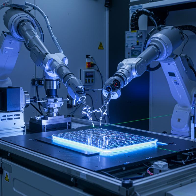
Wafer Processing and Bonding Done with UV Light Could
Imposing a Complex Layer Over the Wafer Surface Photolithographically
With photolithography, advanced patterns are superimposed on wafer surfaces during sequential operations, and the removal is achieved in steps as tiny as a few nanometres.
Processes Done Without Application of Heat
Temperature-sensitive materials like GaAs glasses and other delicate composites stand to gain from stress-free treatment like UV exposure.
Surface Cleaning and Modification
During the coating or bond layers preparation stages, UV cleaning can deactivate surfaces by cutting carbon chains that result in contaminant-free surfaces.
Sustainability and Eco-friendly Innovations
Silicon wafer exposure tools from the last generation utilize devices that employ mercury-free ultraviolet LED technologies. These devices are more eco-friendly because of their lower energy consumption as well as extended lifespans.
Key Functions of UV in Wafer Processing
UV Photolithography
For engraving micro and nano features on the wafers and DUV lithography has greater capability for further size reduction.
UV Wafer Bonding
Utilizes ultraviolet adhesives at fairly low temperatures, which is a must in WLP and MEMS technologies, to bond wafers.
UV Assisted Etching and Dicing
Provides scribing of silicon, sapphire, and glass wafers using UV lasers to enhance edge quality while minimizing debris and improving precision.
Surface Activation
A decrease in adhesive bond energy and surface energy with an increase in interfacial energy causes strengthening of the adhesive bond.
Post Exposure Bake (PEB)
Processes for post-exposure to photoresist strengthen cross-linking of the bonds, reinforcing image definition and improving adhesion and strength overall.
Technical Exposure: UV Systems Applied to Wafer Processing
Just like any other tool used in the semiconductor field, UV systems used for wafer processing require accuracy, reliability, and ecological compliance. They integrate both deep UV (185 nm) and near-UV (405 nm) in addition to exceeding the 20 W/cm^2 exposure intensity threshold needed for modern lithographic techniques and advanced wafer dry cleaning, bonding, and etching processes.
Compared to lasers and steppers, mask aligners possess differing UV wafer exposure methodologies. These systems process silicon, GaAs, glass, and sapphire wafers, provide passive and active temperature control, and prevent overheating through temperature management.
Sources of UV radiation, both passive and active, differ from one another in their intensity and spectrum. These systems are suitable for R&D units as well as for automated and semi-automated production lines due to their partial or full automation capabilities.
What benefits over traditional?
When looking at the benefits of water processing UV and comparing it to traditional thermal or chemical methods, it is clear that the advantages outweigh the disadvantages. First of all, UV WAFE processing improves the existing micro- and nano-fabrication techniques. Integration with UV photolithography systems improves the cumulative accuracy achieved for complex pattern definitions.
- Vertical curing and exposing UV systems vertically boost throughput while addressing cycle time constraints. In turn, this decreases idle time as production efficiency increases and optimizes the volumetric production uptime metrics.
- With these systems not requiring as many bulb replacements, the maintenance and operational lifespan of the bulb-based UV systems increases. When these systems are used together with lower power consumption, they become capable of higher and sustained savings.
- As today’s eco-friendly systems still relate to lower hazard impacts, removal of mercury and other hazardous chemicals makes these systems green. Also, the lower temperature radiation that these ultraclean systems generate sets them below the sensitivity limits for wafers that may be damaged by heat.
- Reduced reliance on wet chemical baths also enhances process cleanliness and results in cleaner yields.
Ultraviolet Treatments of Materials and Substances
Silicon wafers – Most useful for integrated circuits as well as MEMS devices.
Gallium Arsenide (GaAs) – Utilized in radio-frequency and photonic systems.
Glasses and fused silicas – Applied in optical devices, biosensors, and other associated technologies.
Polymer Substrates – Employed within flexible electronics.
Photoresists – Necessary for heliographic and lithographic processes.
Photolithography in MEMS and IC Technologies
In MEMS, with ultraviolet control, it is now feasible to design and fabricate precision movable nanoscale beams, sensors, and even actuators. In integrated circuit technology, multi-layered photomasks are produced by deep UV soft lithography. During the process of urethane polymerization of photopolymers, diepoxy resins, also known as die swell, enhance the bonding of dielectric and metal layers, which improves dielectric and metal layer adhesion.
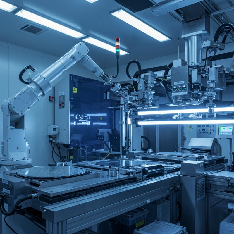
Cleanrooms and automation
Cleanroom class ISO designs have been integrated with new automation features; in addition, UV wafer processing system boundaries are extending. Systems provide:
- Inline automated fume extraction for uninterrupted, continuous synthesis of the wafer.
- Touch panel interfaces.
- Sustained supply and low emission of shielding particles reduce airborne contamination.
- Modular structural design for gradual scaling of production capacity.
- Low emission of contaminating particles.
Buyer’s Guide: Choosing The Best System For UV Wafer Processing
Choosing the right UV wafer will refine a semiconductor company’s speed, accuracy, and efficiency. The most critical considerations during selection include:
• Range of Wavelengths
Confirm that the photoresists and bonding agents used have UV ranges of 185–405nm.
• System Exposure Control Intensity
Ensure varying and preset-patterned parameters have fixed intensity settings and precise dose control.
• Methods of Cooling
Active (liquid/air) and passive (heatsink) must provide adequate overheating protection during extended operational periods.
• Scalability
Research and development begin with benchtop units that advance to inline systems for high-volume production. Custom-engineered systems for production-tailored units are built around specific demands.
• Compatibility With Automation
Evaluate gaps with robotic handlers, conveyors, and cleanroom automation for other systems interfaces without risk of gaps in the automation interface.
Help From Partners and Maintenance Equipment Vendors
For logistical repair and service support, receiving timely aid is greatly valued by vendors. UVET is unmatched in providing high-speed, eco-friendly, state-of-the-art cleanroom compatible UV wafer processing systems for semiconductors. These systems are well-trusted by semiconductor engineers all over the globe because of the trust in the speed and precision of the systems.
Conclusão
As the volume of production rises, the demand for semiconductor UV processing surges. The advantages provided by ultraviolet light in the manufacturing of semiconductors are the precise work enhancement and cost-effective scaling in a clean-standard manner. This precision is achieved with light-assisted bond and etch tiered wafer fabrication. Looking to refine precision for your production? Cutting-edge technology is waiting for you at UVET, where unmatched industry precision is achieved with every UV wafer system layer construction.